
 Imaging IP License
- CMOS Image Sensor IP (Column A/D Convertor, etc)
- CCD Image Sensor IP (PGA, CDS, AFE, etc)
- Image Processing IP (ISP, etc)
- Other CMOS Image Sensor IP
CMOS Image Sensor IP
| IP Name |
Cont. | Format | bit (bit) |
Max Trans Time (uS) |
Column Power Current (uW) |
Column Pitch (um) |
Ana Dig Power Volt (V) |
Spec | Supply Status(nm) | ||||
|---|---|---|---|---|---|---|---|---|---|---|---|---|---|
| 55 | 90 | 180 | |||||||||||
| U | T | J | U | J | |||||||||
| CI00301 | ColumnA/D Converter |
Single Slope |
12 10 |
19 7 |
11uW | 2.2 1.1x2 |
3.3/1.2 | ||||||
| CI00201 | ColumnA/D Converter |
W-SA | 12 | 3.75 (2.75) |
15 | 5.6 2.8x2 |
3/1.8 | ||||||
| CI00101 | ColumnA/D Converter |
Warp Walk |
14 | 30 | 20 | About 7 | 3.3/1.8 |
||||||
| CI00001 | Low Power SenseAMP |
Current Detect |
- | 250 MHz over |
50uA | - | 1.8 Until 1.0 |
||||||
CCD Image Sensor IP
| IP Name |
Cont. | Max Freq. (MHz) |
Typ. Reso. (bit) |
Max Gain |
Gain Step (dB/LSB) |
Input Vcm (V) |
Input Vdif Range (V) |
Pow Volt (V) |
Spec | Supply Status(nm) | ||||||
|---|---|---|---|---|---|---|---|---|---|---|---|---|---|---|---|---|
| 55 | 90 | 130 | 180 | |||||||||||||
| U | T | U | T | U | U | J | ||||||||||
| CI00011 | PGA | 10 | 8 | 4.2 | 0.05 | 0.6 | 1.5 | 3.3 | 90nm |
|||||||
Image Processing IP
| IP Name |
Cont. | Max Input Freq. (MHz) |
Input Density (bit) |
Max Output Pixel (pixel) |
Max Output Frame Rate(fps) |
Spec | Supply Status (nm) |
|---|---|---|---|---|---|---|---|
| CD00011 | Image Signal Processing (ISP) |
150 | 8/10/ 12/14/16 |
1920x1080 | 60 | NDA |
Soft Macro |
| CD00011A | Pre Processing |
NDA |
|||||
| CD00011B | Post Processing |
NDA |
|||||
| CD00011C | Camera Auto |
NDA |
Other CMOS Image Sensor IP
| IP content | Explain |
|---|---|
| Column Amplifier | The circuit composition which coped with each of the one for column A/D converter and global A/D converter. |
| Low Power Counter-Driver & Latch Circuits |
The circuit composition that the latch circuit which is necessary for the integrating A/D converter, and driver of gray-code counter data can be low power. It is especially effective when it is high-speed clock. |
| Ramp Generator Circuits | With the electric current switch type D/A converter format, together, a small area circuit by switched capaciter type. Both can cope with slope valiability. |
| Analog OB Clamp Circuits | The analog OB clamp circuit of the adjusting feedback type an OB pixel signal to the constant level for the format of each column A/D type and global A/D type. |
Original algorithm Proposal of New Type Column ADC
![]() Introduction
Introduction
It is an analog output for the customer that its company is developed as for the commodity that applies CIS (CMOS image sensor) A digital signal of CIS and latter part is processed ISP Isn't Interface a problem of racking one's brains?
Analog Front End?The circuit to be said is one of the very difficult circuits. The load is heavy to develop its company, and unavoidably There might be a case said that cannot help making AFE Chip external, commercializing or it giving up the product development in it because the miniaturization is difficult, too.
Our company was this The custom of an analog circuit As the beginning, it highly accurate of original our company it was high-speed it aimed supplying it to the customer as IP "ASIP" (*1) The development of Column/Parallel ADC began.
By making minutely The processing performance of ISP improves rapidly, and there is a possibility that the output speed of age [dega] and CIS that the application that has not been thought up to now is possible becomes a bottleneck.
The Column/Parallel method made it on a chip by the method that is appropriate for a high-speed reading CIS was adopted, a high-speed taking picture was achieved, and there is an example of the success in the differentiation of the digital camera, too. Our company Column/Parallel ADC can satisfy the demand of the customer who can unite speed-up to making to high resolution by an original "Warp & Wlak" algorithm, and is examining the application of such high-speed signal processing.
The custom that all customers can be satisfied It must aim supplying IP, and, first, the voice must feel free to disregard if it is interested.
(* 1: It is our coinage, and it means Application Specified Intellectual Property. )
![]() Outline of this method
Outline of this method
![]() High speed and high accuracy
High speed and high accuracy
Speed-up and making to high accuracy are one by one united by simultaneous using the comparison method and the Single-Slope method.
![]() The high rank Digiize is one by one done at high speed by comparison method (=Warp), and subordinate position afterwards Digitize "Warp&Walk Algorithm" done in high accuracy by Single-Slope method (=Walk)
The high rank Digiize is one by one done at high speed by comparison method (=Warp), and subordinate position afterwards Digitize "Warp&Walk Algorithm" done in high accuracy by Single-Slope method (=Walk)
![]() “Fine Calibration Technique" to minimize error margin of cooking stove switch of high rank and subordinate position
“Fine Calibration Technique" to minimize error margin of cooking stove switch of high rank and subordinate position
![]() Layout size minimization
Layout size minimization
The circuit element necessary for Column ADC is reduced by doing as not the comparison method one by one and the charge redistribution type of DAC used but the voltage selection type.
![]() It is individual Because it is possible to compose, make it minutely only with the transistor almost the time of Column road Pitch Shrink is easy, and the pixel size is small can the adjustment also to CIS and height ..Sensor Noise.. by [inpuri] of S/N "Double CDS" the peculiarity to Column FPN is minimized.
It is individual Because it is possible to compose, make it minutely only with the transistor almost the time of Column road Pitch Shrink is easy, and the pixel size is small can the adjustment also to CIS and height ..Sensor Noise.. by [inpuri] of S/N "Double CDS" the peculiarity to Column FPN is minimized.
![]() It remains with Analog CDS Clamp Error In the operation of the subtraction "Single-Slope" as "Multi-Slope" with Digitial Domain, it is Averaging Random Noise can decrease.
It remains with Analog CDS Clamp Error In the operation of the subtraction "Single-Slope" as "Multi-Slope" with Digitial Domain, it is Averaging Random Noise can decrease.
![]() Aplication Flexible drive according to Operation Mode
Aplication Flexible drive according to Operation Mode
![]() Application example
Application example
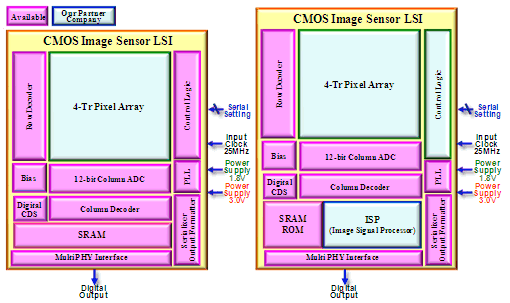
*Serial Interface in accordance doesn't limit it to Multi-PHY ( DPHY & sub-LVDS(DDR) & SMIA CCP2 ).
*MIPI D-PHY, SMIA-CCP2, sub-LVDS, LVDS, and MDDI, etc. can correspond flexibly.
*) No special NDA (Mutual Non-Disclosure Agreement) is required for the content distributed on this website. We are preparing detailed materials to be distributed after the conclusion of NDA.
If you need it, Please contact us from here.